
INTRODUCTION:
Dental implant grafting, also known as the technique of dental prosthesis, has revolutionized the field of restorative dentistry, providing long-term and effective solutions for missing teeth. An implant is a titanium post that is surface-treated to replace the root of a tooth, a material chosen for its exceptional compatibility with human biology. Next, we will delve into the important role of Scanning Electron Microscopy (SEM) in enhancing the effectiveness of the dental implant grafting technique.
Scanning Electron Microscopy (SEM) and stereomicroscopy of dental implant grafts:
Dental implant grafting is a technique to replace the lost root portion, typically made from titanium. This metal is known for its strong biocompatibility, and the human body accepts titanium without adverse reactions, which is crucial for any material integrated into human bone.
To improve the integration capability of the graft, the surface of the titanium screw is intentionally roughened. This structure increases the surface area in contact with the jawbone, enhancing the bone's ability to grow against the surrounding graft tissue. This process, known as osseointegration, is vital for the stability and longevity of the graft.

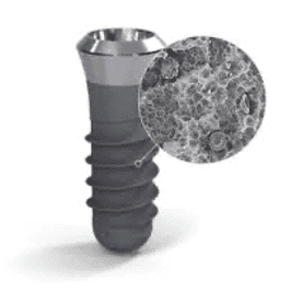
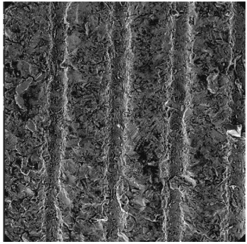
Scanning electron microscopy (SEM) plays a key role in the development and refinement of dental implants. By creating high-resolution images, SEM allows researchers and manufacturers to meticulously analyze the surface roughness of titanium implants. This technology provides detailed images that are crucial for evaluating the effectiveness of surface treatment methods aimed at optimizing the integration of titanium dental roots with the jawbone.
A particularly valuable technique in this context is the use of SEM for stereomicroscopy. By capturing two SEM images at different angles (tilted), it is possible to create a three-dimensional image. This allows us to visualize the surface of the implant in three dimensions, providing a more comprehensive analysis of the surface structure. Such precise measurements are a tool to ensure maximum effectiveness of bone integration.

Advanced SEM models like Semplor NANOS can be integrated with complex analysis software, such as Mountains software. This integration allows for automated and accurate analysis of SEM images. Users can measure, visualize, and quantify surface roughness with unprecedented accuracy and ease, making it an indispensable tool in the quality control of dental implants.
Tilt angle (standard NANOS feature)
Tilt angle -/-15 up to +40 degrees
SE or BS images
Mountains software
TECHNOLOGY:
CONFIGURATION: NANOS is equipped with integrated BSD, SED, EDS, and a tilted stage.
DESIGN: NANOS features a modern, robust design and is constructed with the latest materials and components.
SERVICE: The NANOS design allows easy access for maintenance and upgrades that can be completed at your facility.
POWERFUL: With excellent stability and a compact size, the architecture of NANOS ensures it can be used in non-laboratory environments.
EASY TO USE: In BASIC mode, NANOS will produce results in a short time, regardless of experience. The ADVANCED mode provides additional functionality for detailed analysis.
COST OF OWNERSHIP: NANOS has been designed to keep ownership costs lower than any existing benchtop SEM.
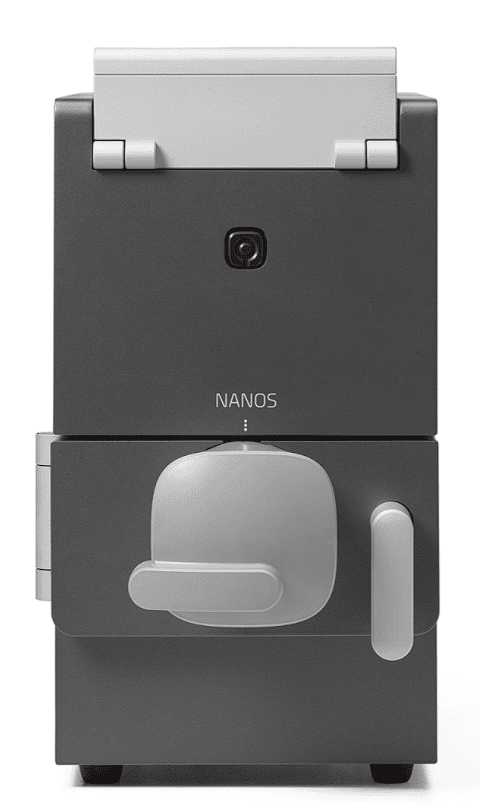
NANOS is a comprehensive benchtop scanning electron microscope (SEM) designed with the latest technology, providing fast and high-quality SEM imaging and elemental analysis. Its design is robust and modern, making it perfect for research & development, education, and industrial use.
Signal Detector:
NANOS comes standard with both a secondary electron detector (SED) and a backscattered electron detector (BSD). The BSD is a 4-quadrant detector with fully controllable independent segments. By using the segments in different combinations, it provides details about the composition or surface structure of the sample, as well as images with 'shadowing effects' by highlighting the surface from multiple angles. The energy dispersive X-ray (EDX) SDD (Silicon Drift Detector) has been installed for elemental analysis.
Elemental analysis:
NANOS is equipped with a fully integrated EDX SDD (Silicon Drift Detector). The operator can choose EDX Point Analysis or activate Elemental Mapping.
Eccentric stage:
The NANOS eccentric stage is truly the only stage of its kind. The motorized XY movement can be controlled through the user interface. Tilting the sample in SEM mode can be done by manually rotating the stage. Thanks to the eccentric design, the sample remains in focus without needing intermediate changes in the SEM settings. The user interface indicates the exact tilt angle. Samples can be tilted up to 55 degrees.
User interface:
SEM is about imaging, and NANOS places imaging at the center of the screen. NANOS is easy to set up, has an intuitive interface, and requires minimal training to start imaging samples. The software offers both a Basic mode for quick and simple SEM imaging and an Advanced mode for in-depth sample analysis. Users have full control of NANOS through a wireless scroll mouse and keyboard and can be set up for remote operation via an iPad or similar device. The Navigation Camera (NavCam) is always on to ensure users know exactly what sample is being measured.
Navigation camera:
When loading a sample, an optical image of the sample is created to serve as a navigation image providing a complete view of the sample. Through the User interface, users can easily navigate the camera over the sample, giving them full control even at high magnifications.
Low vacuum reduces sample discharge phenomena:
Samples are observed in high vacuum SEM (conventional SEM) or in low vacuum (low vacuum SEM). Low vacuum is used to reduce or eliminate the effects of sample charging. When observing conductive samples in high vacuum, electrons accumulate on the sample surface causing charging phenomena. NANOS is equipped with a low vacuum mode to address this.
Electron source:
The electronic heat-emitting source in NANOS is a tungsten filament controlled by an electromagnetic coil lens and an electrostatic deflector. By using the optional 'ECO' setting, the lifespan of the filament can be extended up to hundreds of hours while still producing high-resolution images. Any user can replace the electronic source with a simple alignment tool, ensuring minimal downtime.
Maintenance, Service:
NANOS has been developed with service at its core in its design. The removable electronic boards, modular components, a single control panel, and several moving parts help minimize service requirements. Users can perform many tasks. The unique point of NANOS is that there are no moving parts in the vacuum chamber. Thanks to this smart design, the risk of contamination has been eliminated.