
Electron Beam Lithography (EBL)
Electron Beam Lithography (EBL) is one of the most advanced technologies in the field of microstructure and nanostructure fabrication, widely used in scientific research and modern microchip production. EBL is a "maskless lithography" technique, meaning it does not require a mask, allowing for the direct drawing of extremely small patterns with nanometer-scale resolution on the surface of materials through the use of high-energy electron beams. This article will detail the operating principles of EBL, the structure of the equipment, types of resists, advantages and disadvantages, comparisons with traditional photolithography, practical applications, and future development trends. It also serves as an in-depth resource for readers, researchers, students, and engineers to gain a comprehensive understanding of this special type of equipment.
Before delving into EBL, it is essential to understand why lithography technology plays a crucial role in the semiconductor industry. Traditional photolithography uses ultraviolet light to create microstructure patterns on silicon surfaces. However, the wavelength limit of light makes it difficult to achieve resolutions below several tens of nanometers. Therefore, EBL has been researched and developed as a nano fabrication tool with the ability to surpass the diffraction limit of light, ushering in a new era in microchip technology and nanomaterials.
The basic principle of EBL
The basic principle of EBL is based on the use of an electron beam emitted from an electron gun, which is focused by an electromagnetic lens system and precisely scanned over the surface of the electron resist. When electrons collide with the resist, they cause chemical changes such as polymer scission or cross-linking, altering the solubility of the resist in the developing solution. After the patterning process is complete, the sample is taken for development to remove the altered resist, thereby revealing the desired patterned areas. Subsequent steps may include plasma etching, lift-off, or thin film deposition to create the final structure.
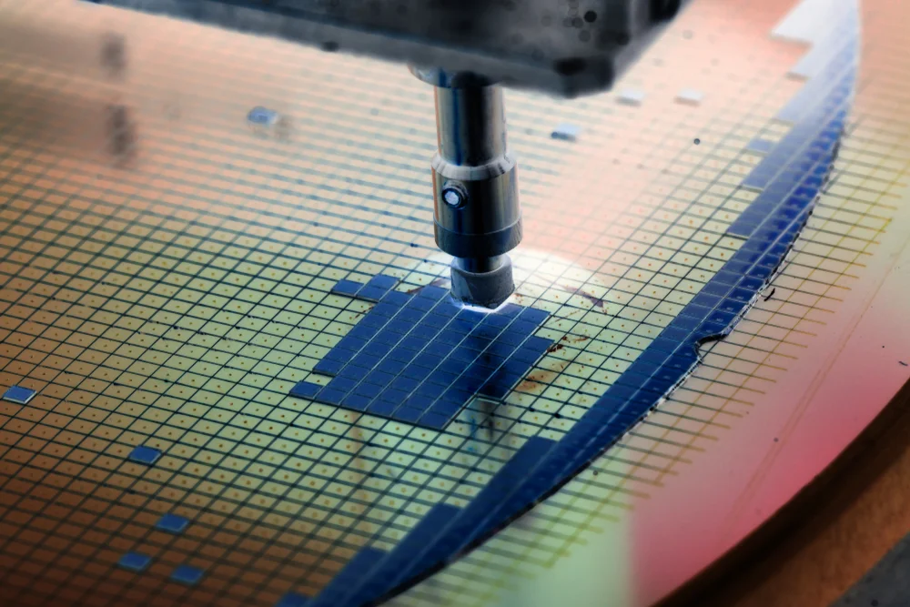
The structure of the electron beam lithography system consists of several key components: an electron source (commonly a thermal cathode or a field emission source), an electromagnetic lens system used to focus and direct the electron beam, a beam scanning and control system, a high vacuum chamber to reduce electron scattering, a high-precision sample stage, and a data processing system that controls the pattern writing process. Thanks to the synchronized coordination of these components, the EBL system can achieve accuracy within a few nanometers, surpassing other fabrication techniques.
Another important component in EBL is the resist material. Among them, PMMA (Polymethyl methacrylate) is the most common resist, operating on the mechanism of polymer chain scission under the influence of electrons, making it easy to wash away the irradiated part. Additionally, there is HSQ (Hydrogen silsesquioxane) – an inorganic resist that operates on the mechanism of cross-linking, creating durable patterns that are well-suited for etching, suitable for applications requiring high precision. Depending on the research goals and specific applications, users will choose the appropriate type of resist to optimize the fabrication process.
Compared to traditional photolithography, electron beam lithography has many superior advantages. First is the extremely high resolution, which can go down to 5–10 nm, while photolithography with deep ultraviolet (DUV) light is limited to about 50–100 nm, and even EUV lithography with a wavelength of 13.5 nm is facing many challenges regarding cost and mass production. Second, EBL is a maskless technology, meaning that patterns can be flexibly changed through software, saving time and costs in mask fabrication as in photolithography. Third, EBL is very suitable for creating complex custom patterns or producing small quantities, especially in scientific research and prototype fabrication. However, the biggest drawback of EBL is its slow speed, as the electron beam must sequentially scan each point on the surface, making the fabrication of large area patterns time-consuming. Additionally, the investment cost for equipment is also high and requires operation in strict cleanroom conditions.
To make it easier to visualize, we can think of EBL as a "nano writing pen" using electrons instead of light. If photolithography is like using a "printing mold" to mass-produce identical patterns, then EBL is more like manual engraving with extremely high precision. Therefore, EBL is often used to create unique nano structures that photolithography cannot achieve.
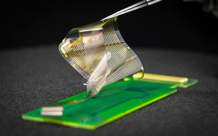
Application in microchip manufacturing
EBL is used to write ultra-small electrode patterns for next-generation transistors, especially in semiconductor research laboratories. Transistors at the nanometer scale can only be studied and tested thanks to EBL's precise patterning capability. This helps scientists validate new ideas before moving to mass production technology using photolithography.
Application in the fabrication of metamaterials
EBL is used to create nano metal networks with exotic structures, allowing for control of light at the nanoscale. These metamaterials can bend light, create optical cloaking effects, or fabricate ultra-small photonic waveguides.
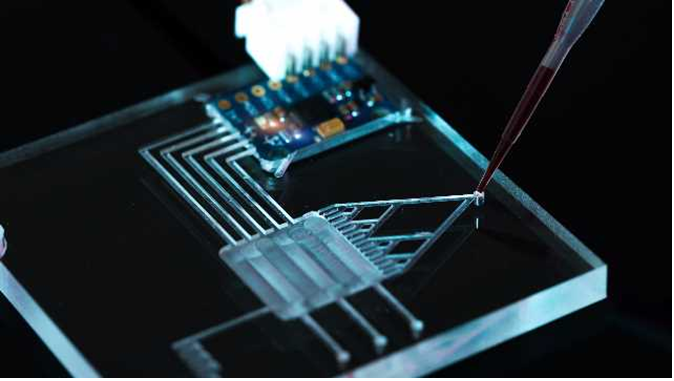
Application in nano biosensors
One of the prominent research directions today is using EBL to create nano electrodes or plasmonic structures that enhance signals in the detection of biomolecules. For example, DNA or protein sensor chips can achieve high sensitivity thanks to the nano structures created by EBL.
Application in optics and plasmonics
EBL enables the creation of narrow nano slits, diffraction grating arrays, or nano metal antennas. These structures are applied in the development of nano light sources, plasmonic lasers, or components in integrated optics.
Application in quantum physics
In research on quantum computers and spin electronics, EBL is used to fabricate quantum dots, nanowires, or complex superconducting circuits. Quantum devices require extremely high geometric precision, and EBL is the only tool that can meet this need in the early research phase.
In addition, EBL is also used to create molds for nanoimprint lithography (NIL) technology. In this method, EBL engraves an initial pattern on a small substrate, which will then be used as a mold for mass replication using nano printing techniques. This is a way to balance the high resolution advantages of EBL with the speed and low cost of mass printing technologies.
Famous manufacturers of EBL equipment around the world include Raith (Germany), JEOL (Japan), Vistec (Germany), and Crestec (Japan). Each company has its own strengths; for example, Raith specializes in EBL systems for academic research with extremely high resolution, while JEOL integrates EBL into scanning electron microscope (SEM) systems to create multifunctional fabrication stations. The price of an EBL system typically ranges from several million to tens of millions of USD, requiring clean rooms and a professional operating team.
Regarding future trends, EBL continues to play an important role in fundamental research and prototype fabrication. In the semiconductor industry, EBL is unlikely to replace photolithography in mass production due to speed limitations, but it plays an essential role in developing new technologies, testing next-generation transistors, and creating initial mold prototypes for replication techniques. Additionally, with the development of quantum computing technology, nano sensors, metamaterials, and integrated optics, the demand for EBL is increasing. Research is also focusing on developing more sensitive resists, parallel electron beam systems to increase pattern writing speed, and integrating artificial intelligence to optimize the lithography process.
Looking back, it can be seen that EBL has been, is, and will continue to be one of the most powerful tools in the field of nanofabrication. From creating ultra-small circuits, complex photonic structures to next-generation biosensors, EBL has always proven its irreplaceable role. However, widespread deployment still depends on cost, speed, and automation capabilities. Therefore, EBL often goes hand in hand with photolithography and other fabrication technologies, creating a complete ecosystem serving both research and industry.
In summary, electron beam lithography is currently the highest resolution nanofabrication technology, allowing for the creation of unique structures that no other method can achieve. Despite existing limitations in cost and speed, EBL remains an indispensable tool in the research and development of microchip technology, nanomaterials, and photonic devices. With advancements in science and technology, we can expect EBL to increasingly play a role in new fields such as quantum computing, nano sensors, metamaterials, and next-generation semiconductor manufacturing.