
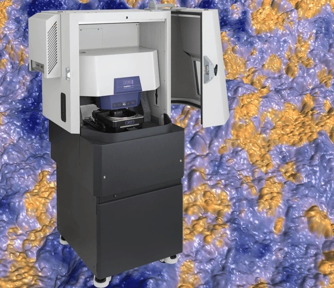
In materials science, powerful microscopy tools are of paramount importance as they provide detailed insights into the complex nature of materials at the microscale. Among such tools, atomic force microscopy (AFM) stands out as a powerful technique that overcomes the limitations of traditional methods by providing high-resolution images and properties at the nanoscale.
This article discusses the application of AFM in topographical and surface morphology analysis, assessing mechanical properties, and mapping chemical composition.
Introduction to AFM
AFM differs significantly from traditional microscopy techniques because it does not illuminate the sample surface with light or electrons to create its images. Instead, AFM uses a sharp probe while scanning the sample surface, measuring the small forces acting between the probe and the sample surface. This measurement translates into information about the properties of the sample.
AFM can analyze a wide variety of materials, both conductive and non-conductive, in various environments, including air, liquids, and even extreme temperatures.
Topographical and surface morphology analysis
AFM helps investigate surface features by generating high-resolution three-dimensional (3D) images that reveal surface roughness, topography, and morphology. This is crucial for understanding the interaction of materials with their environment, such as wear resistance, adhesion properties, and the ability to self-assemble into complex structures.
For example, AFM can be used to analyze the surface structure of implantable devices or drug delivery devices, aiding in the design of biocompatible materials with optimal performance.
Analysis of polymer-DNA morphology using AFM: A case study
A 2022 study investigated the morphology of conductive polymers (polyimidazole, polyindole, and polypyrrole) molded by DNA using AFM. The researchers found that polyimidazole/DNA exhibited a spherical and agglomerated nanostructure, while polyindole/DNA displayed a dense network of nanowires in concentrated form and individual strands in diluted samples.
Polypyrrole/DNA shows various morphologies, including bare DNA strands, well-bonded polymer nanomaterials, and high-density films. Statistical analysis indicates that the dominant nanowire diameter is 3-4 nm. Despite the differences, all polymers demonstrate potential applications in nanoelectronic devices and chemical sensors due to their uniform, smooth, and continuous morphology, suitable for alignment on nanoelectrodes.
This comparative AFM study enhances the understanding of the morphology of polymer/DNA molded nanowires and their potential applications.
Evaluation of mechanical properties
High-speed AFM provides surface imaging and can assess the mechanical properties of materials at the nanoscale. Different AFM modes are used to measure properties such as elasticity, hardness, and adhesion force, helping to understand how materials respond to stress and strain at the nanoscale as well as predict their bulk behavior.
AFM-based input characteristics
In a study Recently, researchers have studied a method for assessing the area of nano sensor devices by using AFM to analyze the plastic traces caused by indentations. The study focused on using indium as a calibration material and conducting nano indentation tests using AFM imaging on indium samples.
The results show that the AFM-based method provides an effective and low-cost means to evaluate the area profile of the nano probe, particularly at heights below 200 nm. Researchers successfully described the geometric shape of the indentation at the nano level by indirectly calculating the expected effective footprint areas.
This approach offers a promising alternative to electron microscopy-based techniques, with advantages in cost-effectiveness, ease of implementation, and rapid data processing. The study highlights the potential of AFM in accurately assessing mechanical properties, emphasizing its importance in nano mechanics research.
Chemical composition mapping
AFM can be integrated with other techniques to further expand its applications.
For example, scanning probe microscopy (SPM) combined with spectroscopic methods creates a powerful tool for chemical analysis, allowing researchers to visualize topography and identify different materials present in the sample at nano resolution.
AI & Machine Learning eBook in the industry
 A compilation of interviews, articles, and top news from the past year.
Other techniques, such as scanning tunneling microscopy (STM) or spectroscopy with scanning probe microscopy (S-SPM), can be combined with AFM to map the chemical composition of the sample surface.
To further expand the applications of AFM, researchers are continuously striving to develop new methods to overcome the limitations of conventional AFM.
For example, in a study recently, researchers developed coated active scanning probes for AFM to enable topographical imaging in turbid liquid environments. Traditional AFM systems rely on the deflection of an optical beam, limiting imaging in transparent environments. The newly developed probes feature piezoelectric deflection sensors and thermal actuators, eliminating the need for optical systems and allowing imaging in turbid liquids.
These probes withstand harsh chemical conditions and have been successfully tested in various turbid liquid environments. The research demonstrates the potential of coated active probes to observe samples in their natural environments, paving the way for new AFM applications in biology, chemistry, and materials science.
Future Directions and Innovations
Innovations in AFM equipment, such as faster scanning speeds and higher sensitivity probes, will further enhance the capabilities of AFM in studying dynamic processes. For instance, combining AFM with advanced spectroscopic methods could provide real-time information about the chemical composition of materials and their responses to external stimuli.
AFM can also aid in the design of biocompatible materials for implants and prosthetics by providing details about their interactions with biological systems at the nanoscale.
AFM can also be used in 3D printing; by analyzing the surface morphology and mechanical properties of the printed materials, researchers can refine the printing process and ensure functional, high-quality structures.
As these innovations continue to develop, the role of AFM in materials science will become even more comprehensive.